
Ilan Ben-Yaacov, Ph.D
Principal IP Technologist
University of California Santa Barbara, Santa Barbara, CA
● Ph.D, Electrical and Computer Engineering
● MS, Electrical Engineering
● BS, Physics
Ilan has over 20 years of semiconductor research, teaching, and industry experience as an innovator and thought leader resulting in 21 patents and 10 technical publications. His doctoral research was directed at designing, fabricating, and testing GaN-based HEMTs and CAVETs for power switching applications. Ilan assisted with writing the graduate textbook Semiconductor Device Physics with Professor Umesh Mishra (UC Santa Barbara) and Professor Jasprit Singh (University of Michigan). He has extensive industry experience in Ga-N based semiconductor devices and modules, and teaches semiconductor materials processing & device fabrication courses at the University of California, Santa Barbara.
Ilan works with patent attorneys to develop strategic patent portfolios, investigate patent assertions, and perform IP due diligence for semiconductor device companies.
Representative Semiconductor & Patent Experience
Device Level Research
- Researched & published first reported demonstration of AlGaN / GaN current aperture vertical electron transistors.
- Epitaxial growth of III-Nitride semiconductors by metal organic chemical vapor deposition (MOCVD).
- DC and small-signal RF characterization of CAVETs, extraction of small-signal equivalent circuit.
- Design, fabrication, and characterization of nitride-based high electron mobility transistors (HEMTs) and CAVETs.
- Grew materials using MOCVD, designed & fabricated all devices, and performed device electrical characterization.
- Fabrication equipment included stepper lithography, RIE, ICP, e-beam evaporation, Sputtering, PECVD, and RTA.
- Design tools included Tanner L-Edit, SRIM (ion implant simulation), and 1D Poisson solver.
Semiconductor Theory & Practice - University Instructor
- Semiconductor device processing. Intensive theoretical and laboratory instruction in solid- state device and integrated circuit fabrication. Topics include semiconductor material properties and characterization; phase diagrams; diffusion; thermal oxidation; vacuum processes; thin-film deposition; and canning electron microscopy. Both gallium arsenide and silicon technologies are presented.
- Solid-state electronic device structures. Electrons and holes in semiconductors; doping (P and N); state occupation statistics, transport properties of electrons and holes; P-N junction diodes; I-V, C-V, and switching properties of P-N junctions; and introduction of bipolar transistors, MOSFET’s and JFET’s.
- Semiconductor-based circuit design. Theory, fabrication, and characterization of solid state devices including P-N junctions, capacitors, bipolar and MOS devices. Devices are fabricated using modern VLSI processing techniques including lithography, oxidation, diffusion, and evaporation. Physics and performance of processing steps are discussed and analyzed. Design, simulation, fabrication, and characterization of NMOS integrated circuits. Circuit design and layout is performed using commercial layout software. Circuits are fabricated using modern VLSI processing techniques. Circuit and discrete device electrical performance are analyzed.
- Introduction to patents. Provides emerging inventors, entrepreneurs, and scientists with a working knowledge of intellectual property (patents, copyrights, trademarks, and trade secrets), with the main focus being on patents. Covers the basic functions of patents, structure of patents, and patent prosecution.
Patent Portfolio Development, Diligence and Licensing
- Developed semiconductor patent portfolio with device level inventions for a California startup.
- Prepared 30+ patent applications and 200+ office action responses for review and filing by outside counsel.
- Semiconductor patent drafting and prosecution related to III-Nitride (Al, In, Ga) semiconductor materials and devices with unique combination of physical properties that guarantee demand in modern microelectronics and optoelectronics, such as nitride-based enhancement mode high electron mobility transistors (HEMTs) to carry large currents, support high voltages and to provide very low on-resistance and fast switching times; semiconductor heterostructure diodes with low on-resistance, high breakdown voltage, and low reverse leakage currents; and enhancement-mode GaN-based III-Nitride high electron mobility transistors.
Research Publication
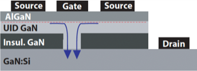
AlGaN / GaN CAVET & Epitaxial Growth of III-Nitride Semiconductors
U.S. Patent 8,519,438
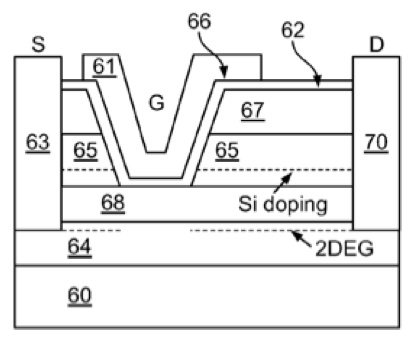
Nitride-based Enhancement Mode
High Electron Mobility Transistors
U.S. Patent 7,898,004
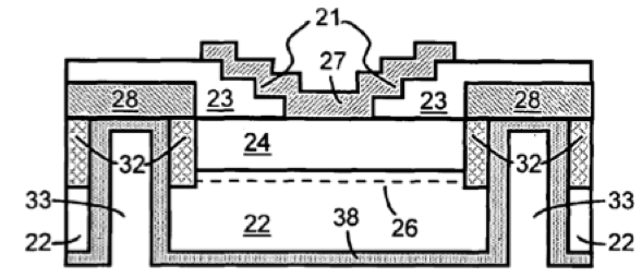
Semiconductor Heterostructure Diodes
with Low On-resistance, High Breakdown Voltage, and Low Reverse Leakage Currents
U.S. Patent 7,851,825
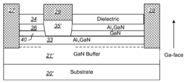
Enhancement-mode GaN based III-Nitride
High Electron Mobility Transistors