Tom Yamashita, Ph.D
Principal IP Technologist
Stanford University, Palo Alto, CA
● Ph.D, Materials Science and Engineering
● MS, Materials Science and Engineering
● BS, Chemistry
Tom has over 30 years of materials science research, commercialization, and industry experience as an innovator and thought leader resulting in 25 patents and 40 technical publications. Tom is passionately dedicated to helping inventors translate their complex inventions into clear and concise intellectual property protection in the field of materials science, fabrication & processing technologies. While completing his doctoral research at Stanford, Tom was invited by Professor William Shockley, Nobel Prize winner for the invention of transistor, to present his doctoral research results. Tom was recruited while a graduate student at Stanford to design and lead the materials science research, development, and manufacturing of a startup business for three decades, during which the startup became a public company and was acquired for $1B by a fortune 100 company.
Tom works closely with patent attorneys on global patent portfolio strategies and development, patent investigation, licensing and litigation matters, as well as M&A diligence, acquisition agreements, and post-acquisition technology integration.
Representative Materials Fabrication & Patent Experience
Materials Research and Manufacturing Processes
- One of the first researchers in the world to produce atomic resolution video recording of dislocation reactions in cadmium telluride (CdTe) by high resolution TEM. Invited by Professor William Shockley, Nobel Prize winner for the invention of transistor, to present the research results directly to him at Stanford University. Recruited from Stanford to lead new pioneering magnetic recording materials R&D for Silicon Valley startup Komag (later $1B public company).
- Researched new material properties / structures based on chemistry, physics, and engineering science for higher density storage devices. Advanced materials science knowledge includes magnetic materials, semiconductor materials (Si, GaAs, CdTe, CdS, and HgCdTe), thin films, photovoltaics, ceramics, and carbon nano-materials including nano-tubes and graphene.
- Conducted high resolution transmission electron microscopy (HRTEM) investigation of CdS/CdTe heterojunction interfaces, an important structure in thin film solar cells. Setup analytical transmission electronic microscopy (TEM) facility at HP Palo Alto Laboratory for materials characterization. Participated in the investigations of Si device failures, GaAs MBE structures, optical fiber materials, oxygen defects in silicon, and analysis of experimental perpendicular magnetic recording structures. Investigated crystalline defects in various CdTe-based materials, including HgCdTe which have applications as sensors, photovoltaics and other optoelectronic devices.
- Equipment & process development of thin films using physical vapor deposition (PVD), chemical vapor deposition (CVD), plasma enhanced chemical vapor deposition (PECVD), inductively coupled plasma (ICP), and ion beam deposition (IBD) processes.
- Reactive ion etching (RIE) processes and manufacturing equipment. Ultra violet (UV) treatment of materials, UV curing and surfaces modification, molecular reaction enhancement, and developing manufacturing equipment with a vendor to do the same. Leveraged silicon chemo-mechanical polishing (CMP) process to develop equivalent process for hard disk substrate planarization.
- Precision polishing process development, materials and their equipment. Substrate and wafer cleaning processes and their equipment. High performance lubricants, and method of application. Design and build complex sputter, PVD/PECVD tools for R&D and for large scale manufacturing. Materials characterization and metrology techniques, TEM, Auger, ESCA/XPS, SIMS, RAMAN, GCMS, FTIR.
Patent Portfolio Development and Licensing
- Managed patent portfolio development program as Chief Technology Officer of Komag, Inc.
- Led invention review boards to identify and prioritize inventions for global patent filings.
- Worked with intellectual property licensing and litigation teams to evaluate and defend products against asserted patents, and negotiate licenses.
Research Publication
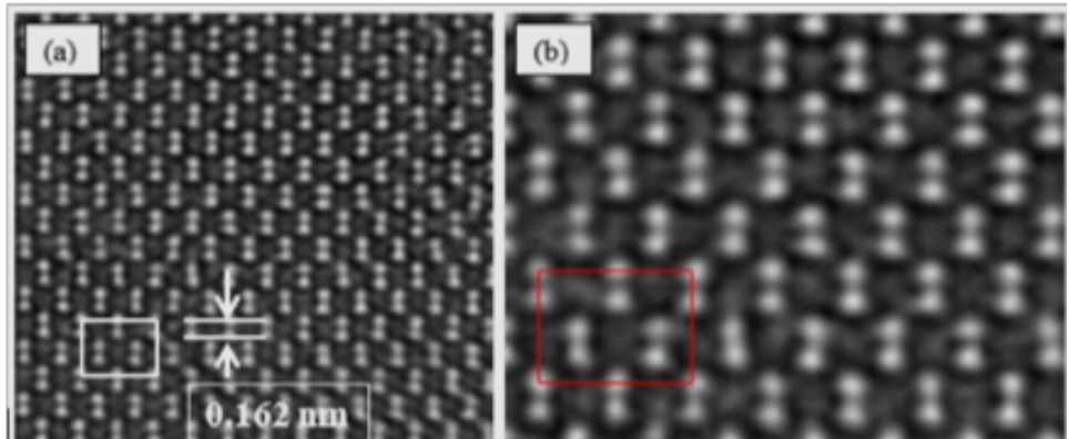
Experimental Atomic Resolution Image of CdTe Crystal in the (110) Orientation.
Research Publication
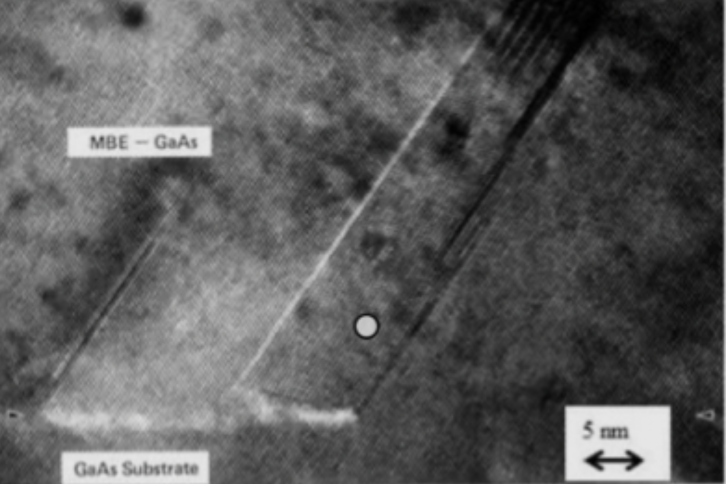
High resolution TEM micrograph of molecular beam epitaxy GaAs / GaAs substrate interface
Research Publication
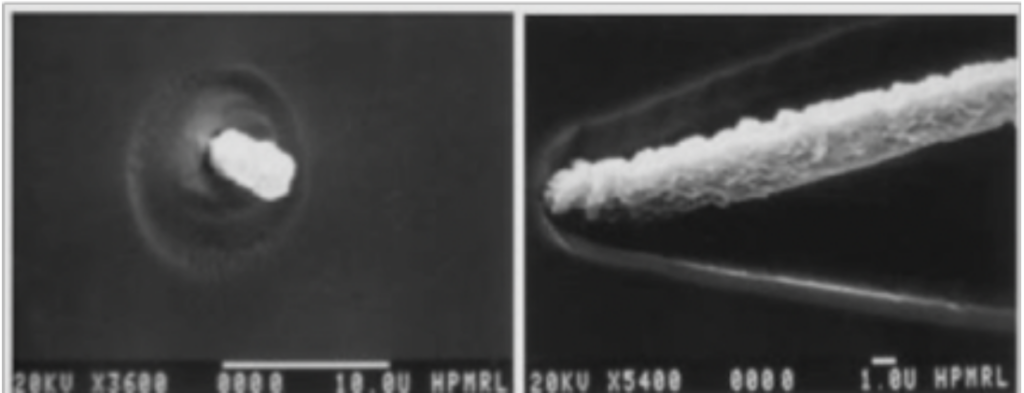
SEM micrograph of hexagonal phase GaAs whiskers on molecular beam epitaxy GaAs film
Materials Research
- One of the first researchers in the world to produce atomic resolution video recording of dislocation reactions in cadmium telluride (CdTe) by high resolution Invited by Professor William Shockley, Nobel Prize winner for the invention of transistor, to present the research results directly to him at Stanford University.
- Recruited from Stanford to lead new pioneering magnetic recording materials R&D for Silicon Valley startup Komag (later $1B public company)
- Researched new material properties / structures based on chemistry, physics, and engineering science for higher density storage devices
- Advanced materials science knowledge includes magnetic materials, semiconductor materials (Si, GaAs, CdTe, CdS, and HgCdTe), thin films, photovoltaics, ceramics, and carbon nano- materials including nano-tubes and
- Conducted high resolution transmission electron microscopy (HRTEM) investigation of CdS/ CdTe heterojunction interfaces, an important structure in thin film solar cells
- Setup analytical transmission electronic microscopy (TEM) facility at HP Palo Alto Laboratory for materials Participated in the investigations of Si device failures, GaAs MBE structures, optical fiber materials, oxygen defects in silicon, and analysis of experimental perpendicular magnetic recording structures
- Investigated crystalline defects in various CdTe-based materials, including HgCdTe which have applications as sensors, photovoltaics and other optoelectronic devices
Manufacturing Process Development
- Equipment & process development of thin films using physical vapor deposition (PVD), chemical vapor deposition (CVD), plasma enhanced chemical vapor deposition (PECVD), inductively coupled plasma (ICP), and ion beam deposition (IBD) processes
- Reactive ion etching (RIE) processes and manufacturing equipment
- Ultra violet (UV) treatment of materials, UV curing and surfaces modification, molecular reaction enhancement, and developing manufacturing equipment with a vendor to do the same
- Leveraging silicon chemo-mechanical polishing (CMP) process to develop equivalent process for hard disk substrate
- Precision polishing process development, materials and their equipment
- Substrate and wafer cleaning processes and their equipment
- High performance lubricants, and method of application
- Design and build complex sputter, PVD/PECVD tools for R&D and for large scale manufacturing
- Materials characterization and metrology techniques, TEM, Auger, ESCA/XPS, SIMS, RAMAN, GCMS, FTIR
Experimental atomic resolution image of CdTe crystal in the (110) orientation.
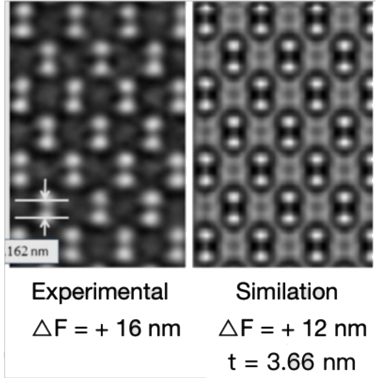
Computer simulation of atomic resolution the experimental images
High resolution TEM micrograph of molecular beam epitaxy GaAs / GaAs substrate interface
SEM micrograph of hexagonal phase GaAs whiskers on molecular beam epitaxy GaAs film

