Lauren Palmateer, Ph.D
Principal IP Technologist
Cornell University, Ithaca, New York
● Ph.D, Electrical Engineering
Monmouth College, West Long Branch, New Jersey
● BS, Electronic and Microwave Engineering.
Lauren has over 30 years of semiconductor advanced research, breakthrough technology & product development, and commercial manufacturing as an innovator, technologist, and thought leader for disruptive products enabling new markets at pioneering research organizations. Her semiconductor research work included (i) supporting Nobel Prize laureate and president of Bells Lab Research in the field of gallium arsenide (GaAs) monolithic microwave integrated-circuits (MMIC) for high frequency quasi-optical detection systems, (ii) doctoral and post-doctoral research in gallium arsenide transistors for high frequency device applications at Cornell, the Paris Observatory, and Thomson-CSF, and (iii) key member of breakthrough technology and product research teams at IBM Watson Research. Lauren expanded her research work to include new semiconductor applications for startup divisions involving Xerox Parc, Seagate Corporation, Qualcomm, and MIT. She is also an entrepreneur and recognized innovator in the field of non-invasive electronic, bio-photonics therapeutic technology. Lauren has over 30 patents and 75 technical publications, and her contributions in microelectronics has been recognized in the Springer Book Series of Women in Microelectronics.
Lauren leverages her deeply rooted semiconductor research background to provide expansive patent engineering & analytics for high stakes invention mining and prior art searches, and to support patent attorneys on patent licensing, pre-litigation, and litigation matters in the semiconductor industry.
Representative Semiconductor & Patent Experience
Equipment & Device Level Research
- GaAs and related III-V semiconductor growth, fabrication and device implementation of (i) High Mobility Electron Transistors (HEMTs) and (ii) AlInAs/GaInAs/InP Modulation Doped Field Effect Transistors (MODFETs) for high speed analog and microwave devices, mixed signal semiconductor components, and optical subsystems.
- DC and small-signal RF characterization of III-V transistors on InP substrates for high- speed microwave applications. Electron transport properties analysis and implementation in microwave device HEMTs and MODFETs, Thin Film Transistors (TFTs), and Micro-electrical Mechanical Systems (MEMS).
- Epitaxial growth of molecule beam epitaxy (MBE) crystal growth of GaAs and related compounds to compete with SiGe as the semiconductor material for achieving target transistor performance.
- Development and characterization of thin film transistors on large area glass substrates for first color laptop flat panel liquid crystal display (LCD) ThinkPad at IBM Watson Research: (i) SiGe thin films in TFTs and displays; (ii) optical display measurements; (iii) manufacturing transfer of processes, test and measurement to joint IBM Toshiba DTI manufacturing facility in Japan; amorphous silicon germanium (a-SiGe:H); and (v) integration of black matrix (BM) in active-matrix liquid-crystal displays (AMLCDs).
- Designed MEMS devices for reflective displays and manufactured iMoD displays as a MEMS-based reflective display technology and array architecture to compete with LCD technologies. Installed and qualified large scale manufacturing equipment for Amorphous Silicon (a-Si) TFT technology: (i) large-scale manufacturing deposition equipment for thin film transistors on glass and flexible substrates; (ii) materials analysis and device level measurement; and (iii) LCD, organic light emitting diode (OLED) and display technologies manufacturing thin film deposition equipment for use and design of OLED and MEMS packaging on large area glass.
- Developed micro display design and fabrication of liquid crystal on silicon (LCOS) to achieve higher transistor / pixel density required for head mounted displays such as used in augmented or virtual reality (AR / VR) applications.
- Device / large scale packaging processes and equipment designs for (i) sensitive electronic components such as displays (MEMS, LCOS, OLED), light emitting diodes (LEDs), solar cells; and (ii) other components with hermetic applications requiring near zero parts per millions (PPM) moisture such as militarized packaging for discreet telecom devices and tunable lasers (hardness and measurement, materials selection and qualification).
- Packaging processes includes (i) interconnect packaging of fine pitch electronic interface to glass (e.g., bonding with anisotropic conductive film (ACF)); (ii) backend component-level structure such as backlights, touchscreens, and digital medical X-ray imaging (amorphous silicon arrays); and (iii) roll-to-roll (R2R) flexible electronics.
Patent Engineering & Analytics
- Harvest inventions for new product research & designs from cross-functional engineering teams.
- Competitive landscapes analytics to identify industry gaps and opportunities for strategic invention and patent portfolio development, and patent acquisitions to support licensing program.
- Patent portfolio analytics with value rankings to support licensing or acquisition diligence based on claim quality (e.g, prior art, validity, enforceability, design alternatives) and business impact (e.g., market size, differentiation, exclusivity, licensing).
- Prior art database searches and analytics showing technical differences or similarities between a prior art reference document and an invention disclosure (patentability) or a patent of interest (validity).
- Reverse engineering of target products to identify technical differences or similarities between the target product and a patent of interest to support high stakes licensing programs and potential litigation claims.
Representative Patents and Technical Publications

Hybrid Drive Writing Copy of Data to Disk when Non- volatile Semiconductor Memory Nears End of Life
US Pat. No. 8,825,977

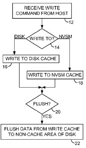
Hybrid Drive Comprising Write Cache Spanning Non- volatile Semiconductor Memory and Disk
US Pat. No. 8,639,872

Hybrid Drive Converting Non-Volatile Semiconductor Memory to Read Only Based on Life Remaining
US Pat. No. 9.146,875

CVD / PVD for Thin Film Layer Fabrication
US Pat. No. 6,008,969

Energy Assisted Magnetic Recording Device
Physics in Canada Journal / Vol 67, No. 1

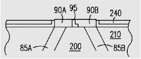
Magnetic recording transducer fabrication with dry etching such as RIE or IBE processes
US Pat. 6,008,969
Materials Fabrication
- Thin film materials design and fabrication for magnetic sensor and storage devices
- Wafer fabrication processes for magnetic field sensor and transducer structures, die test sites and air bearing surfaces
- Chemical vapor depositions and physical vapor depositions for thin film material layers of the storage transducer structure
- Integration of photonic devices (laser diodes, wave guides and photo detectors) into Energy Assisted Magnetic Recording head structures
- Micro-electromechanical systems (MEMS) fabrication of sensors and actuators for storage systems
Electronic Devices
- Solid state memory devices to support system demands for lower power, enhanced reliability, higher storage density, and faster computing
- System-on-Chip controller architecture with microprocessor, read/write channel, encryption, and error checking and correction functions
- Pre-amplifier device design to process and enhance read and write signals between sensors and controller electronics
- Power driver electronics and embedded servo systems to power and control electro-mechanical devices and storage systems
- Interface electronics (PATA, SATA, SCSI, PCIe, NVMe, USB) for communicating with host device
- Non Volatile Memory (3D NAND, MRAM, RRAM) technology research and valuations for multiple joint venture and acquisition deal agreements
- Optimization of tribological interface between air bearings and storage medium to ensure reliability & performance (electrical, mechanical, chemical interface)
System Integration
- Embedded system designs with integrated controller electronics, memory devices, firmware functions
- Solid State Drive and Hard Disk Drive design optimization and integration for enterprise servers, cloud data centers, and client desktop / mobile computing applications
- Network Attached Storage (NAS), Secure Content Digital Video, Hybrid and Tiered Storage Systems
- Integrated firmware design optimization based on application, performance level and reliability requirements including logical-to- physical address conversion, wear leveling, power management, caching algorithms, and SMART algorithms, and bad-block management


